
On July 7, 2023, the 5th Asia-Europe Silicon photonics Symposium and Course was held in Haining International Campus of Zhejiang University. This seminar and training course is jointly organized by Zhejiang University, Ghent University, Belgium, and ePIXfab, Europe. Co-organized by Ghent University-IMEC Photonics Research Team, College of Optical Science and Engineering, Zhejiang University, International Joint Center of Optoelectronic Technology, MOST, China, Joint International Research Laboratory of Photonics, MOE, China, International Research Center of Advanced Photonics, Zhejiang University, State Key Lab. of Extreme Photonics and Instrumentation, China, Research Center of Intelligent Chip and Device, Zhejiang Lab, China.
The organizing committee of the seminar and training course is composed of six organizers, including Academician Roel Baets, Professor at Ghent University -IMEC and President of ePIXfab. And invited 18 experts and scholars from Zhejiang University, Ghent University in Belgium, Eindhoven University of Technology in the Netherlands, University of Southampton and other universities and research institutes around the world, as well as CUMEC, China, Luceda, China, Intel in the United States, Belgium IMEC and other silicon photonic domain enterprises to carry out the theme of academic reports and cutting-edge technology seminars.


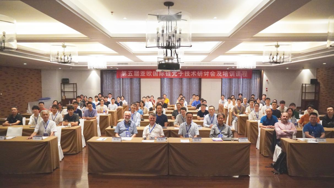
The seminar was officially opened on the morning of July 7 in the Juanhu Hall of Yuanzheng Hotel, Haining International Campus, Zhejiang University. Professor Dai Daoxin, Dean of College of Optical Science and Engineering, Zhejiang University, delivered a speech and a report, and Liu Liu, Professor of College of Optical Science and Engineering, Zhejiang University, presided over the seminar.
The three-day event consists of two sessions: training courses and technical seminars. The training course is presented in the form of academic reports, mainly focusing on the frontier progress, advanced manufacturing process, unique design and other aspects of silicon photonics and integrated photonics, and introducing the present situation and future development direction of science and technology in this field. The technical seminar mainly focuses on the mature silicon photonics technology at the present stage and the multi-class silicon photonics flow plate service for customers, and provides ideas and development direction for promoting the practical and industrialization process. This forum through the combination of online and offline theme report, and with the form of on-site discussion, through the two links complement each other, the development path of silicon photonics and integrated photonics is deeply discussed.
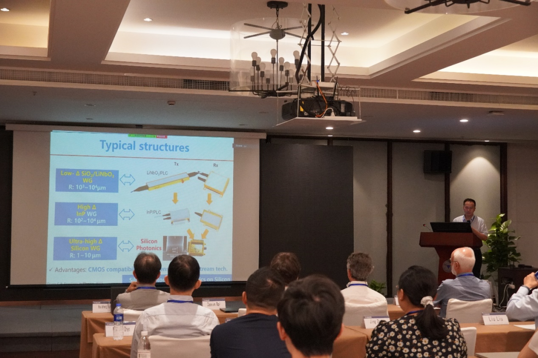

In the three-day academic course from July 7 to 9, senior experts and scholars from Belgium, United States, United Kingdom, Netherlands, Japan and domestic top universities and research institutions made detailed reports on the research directions, platforms and processes of their respective universities and institutes in silicon photonics, as well as the multi-functional units or integrated devices realized on each platform.
During the course, the integration advantages and advanced devices of heterogeneous integration process and silicon nitride platform in Ghent University, Belgium, the design and experimental verification of various cutting-edge silicon based modulators in University of Southampton, the integration technology of indium phosphide platform in Eindhoven University of Technology, the technical route and development direction of 800G optical transceiver in Intel Research Institute, and other universities and research institutes of their own characteristic platforms and work are introduced.
The participating experts gave their respective understanding and solutions based on silicon optical design concept, material platform, manufacturing process, test platform, CMOS compatibility, and practical large-scale production, and discussed the advantages and disadvantages of different platforms and the development prospects of platform crossing in detail through online and offline Q&A dialogue.


From the morning of July 7th to the afternoon of July 8th, the two-day academic seminar was held. The organizers invited well-known experts in the field from various enterprises and universities at home and abroad to share the current application, challenges and future development trends of silicon photonics with many participants.


