
Research Background
In recent years, silicon photonics technology has developed rapidly and has important application potential in the fields of optical interconnection, optical computing, and optical sensing. However, due to the limitations of silicon materials, there are still huge difficulties in the realization of active devices in pure silicon systems. In recent years, two-dimensional materials have received widespread attention for their unique and excellent optoelectronic properties, and are compatible in process, providing an attractive solution for silicon-based active devices. Recently, Professor Dai Daoxin’s team was invited by "Nanophotonics" to write a long review paper on the topic of "Hybrid silicon photonic devices with two-dimensional materials", focusing on the discussion and analysis of silicon-two-dimensional material photodetectors and optical switches/optical modulations. The development status and existing problems of the device, and prospects for its future development.
Summary
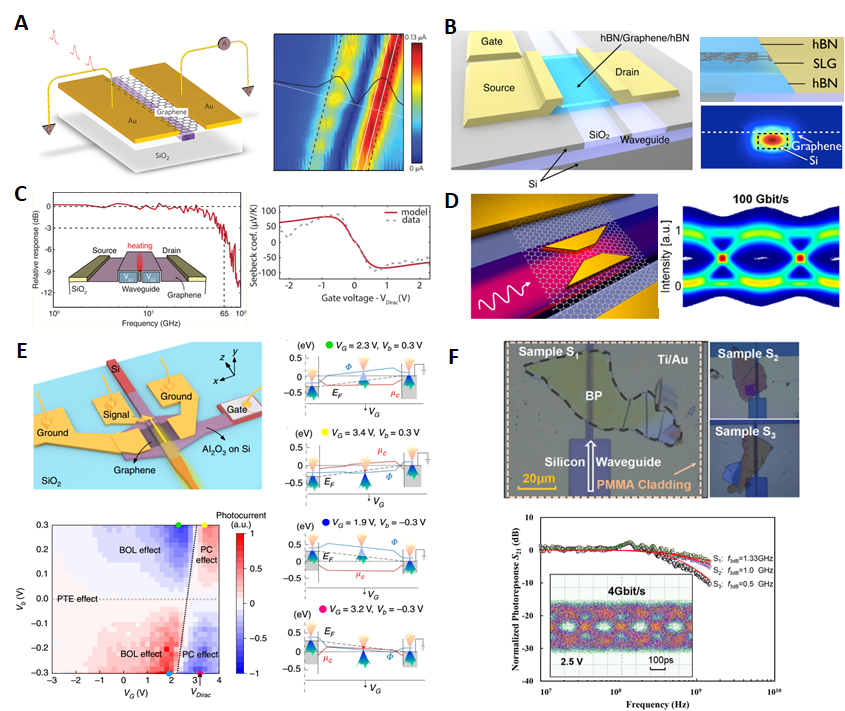
In this paper, author have given a review on recent progresses of hybrid silicon photonic devices with 2D materials for photodetection and optical modulation for the wave-length-bands from UV to MIR. As demonstrated previously, 2D materials provide new opportunities for realizing various active photonic devices on silicon owing to their extraordinary optoelectronic properties. In particular, the light–matter interaction can be enhanced greatly and easily when merging 2D materials with silicon photonic waveguides and cavities. In this way, the interaction length between the 2D materials and the lightwave propagating along the waveguide can be extended very effectively, which is really important for realizing high-performance silicon photonic devices.
Publishing Information
Related results were published in "Nanophotonics" (PhD student Li Jiang is the first author), [Jiang Li, Chaoyue Liu, Haitao Chen, et al. Hybrid silicon photonic devices with two-dimensional materials. Nanophotonics (2020). DOI: 10.1515/nanoph -2020-0093] The above work was funded by the National Science Fund for Distinguished Young Scholars and the National Key Research and Development Program.
Full paper download address:
https://www.degruyter.com/document/doi/10.1515/nanoph-2020-0093/html


